
Palo Alto/ Bhubaneswar: The Government of Odisha delegation which is now in the Silicon Valley USA today engaged in a series of discussions with high-ranking officials of multiple leading business organizations.
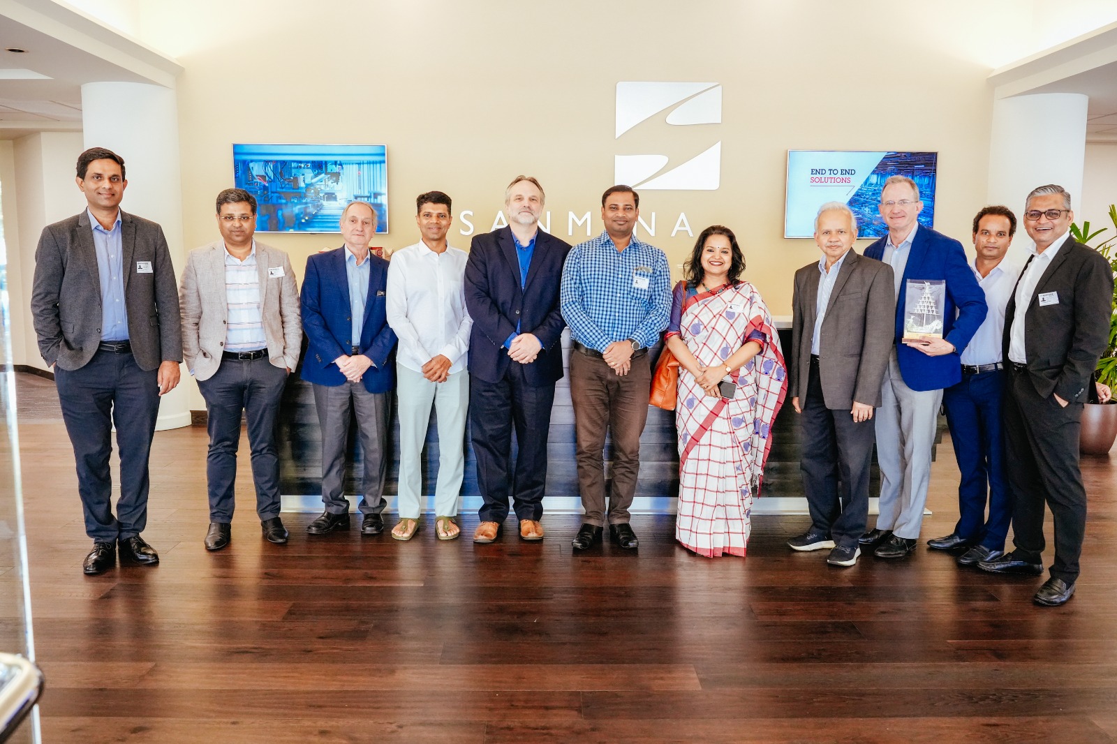
In the first focused meeting of the day, the delegation visited the manufacturing site of Sanmina Corporation, and met its Co-founder and Chairman-cum CEO Mr. Jure Sola, Senior Vice President Dr. Sundar M Kamath, Senior Vice President Mr. Michael Sparacino,; and Vice President Mr. Bill Pappani. Sanmina Corporation is one of the largest global independent manufacturers of Printed Circuit Boards (PCBs) and a leading electronics services provider that serves Original Equipment Manufacturers (OEMs).
The delegation gave a detailed presentation on Odisha’s industrial ecosystem to the Sanmina team and briefed it on the various incentives available under Odisha’s different policies. Sanmina team was impressed by the support and the generous package of incentives Government of Odisha provides to companies.
The company also gave a presentation to Government of Odisha delegation, providing details of its products and solutions as well as expansion plans. It further added that it is looking favourably at India for expansion and diversification of its global supply base.
The company has expressed its intent to submit a detailed proposal to Government of Odisha at the earliest. The delegation assured all possible support in facilitating the investment journey and highlighted the customized and curated package of incentives which are available based on investment size.
Later, the delegation visited the premises of Palo Alto Networks where it met Mr. Anand Oswal, SVP and GM, and his team. Palo Alto Networks is a leading cyber security firm with global presence, including India. The delegation briefed him on Odisha’s policies and the cyber security initiatives the Government has taken.
The delegation and the Palo Alto team discussed on collaboration opportunities in a range of areas which include providing solutions for a cyber-security focused Centre of Excellence, assistance in developing Odisha’s Cyber Security Policy, and supporting Odisha Cyber Security Operations Centre through automation.
To augment nature conservation efforts in Odisha and adopt best global practices, the delegation met with Mr. George Jacob, President and CEO of BayEcotarium. It is the largest watershed conservation organization in San Francisco and is a combination of institutions, united under one mission to protect and conserve the Bay Area ecosystems.
A range of collaboration opportunities were discussed. BayEcotarium also submitted a Letter of Intent to provide help in establishing a Living Oceanarium and a Sustainable Design Museum in the state. The Oceanarium would be unlike any other conceived both in terms of scale and scope of its physical and virtual footprint. The Sustainable Design Museum will enable Odisha to become a hub for design festivals.
In a meeting at Stanford University, the delegation interacted with the distinguished professor and founder of Rambus, Dr. Mark Horowitz. He founded Rambus which designs, develops, and licenses chip interface technologies and architectures and played an instrumental role in the company’s transformation into a global player. The delegation briefed him on Odisha’s O-Chip program under which infrastructure, design, and training support will be provided to companies and start-ups. Mr. Horowitz’s advisory support, given his vast experience, will greatly aid the development of a semiconductor ecosystem in the state and in the flourishing of Intellectual Property (IP) ventures.
These initiatives will soon transform Odisha into a thriving hub for semiconductor innovation that attracts investments, generates high-value job opportunities, and nurtures the brightest minds.
Comments are closed.