
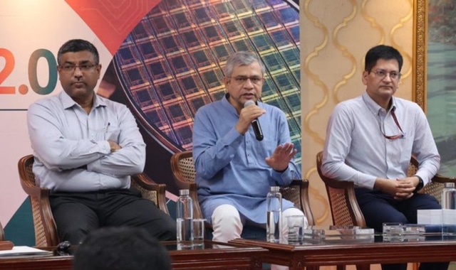
Union Minister for Electronics & Information Technology, Railways and Information & Broadcasting, Ashwini Vaishnaw, today announced the issuance of notifications for all six pillars of the Semicon 2.0 Scheme, marking a decisive step in India’s semiconductor journey.
The scheme, designed to strengthen India’s semiconductor design and manufacturing ecosystem, builds on the success of the first Semicon India Programme. It covers the entire value chain — from chip design and fabrication to packaging, equipment, materials, research, and talent development.
Highlighting India’s rapid progress, Vaishnaw revealed that the country has already trained 85,000 semiconductor engineers in just four years, achieving a target originally set for a decade. He further announced a new goal of developing one lakh additional engineers.
“Close to 10% of the global semiconductor industry’s market will be in India in the coming years,” the Minister said, adding that students from Tier-II and Tier-III cities have already designed more than 250 semiconductor chips, with some projects reaching commercial production in record time.
The six pillars of Semicon 2.0 include:
- Design (IPs, Chips, SoCs, Modules)
- Machines and Materials (manufacturing ecosystem)
- Setting up more Fabs (Silicon, Compound, Display)
- ATMP/OSAT industry (Assembly, Testing, Packaging)
- Research and Development (advanced technologies)
- Talent Development
The scheme is expected to generate 50,000–60,000 direct jobs and will remain open for applications for three years, with projects lasting up to six years. The India Semiconductor Mission (ISM) will act as the nodal agency, overseeing implementation and promoting deep-tech innovation through upcoming awards.