
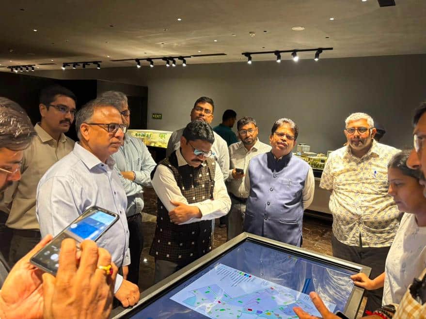
In a decisive step towards positioning Odisha as India’s next semiconductor and technology powerhouse, Electronics and IT Minister Dr. Mukesh Mahaling has completed a high-level visit to Gujarat’s Dholera Special Investment Region and Tata Electronics’ semiconductor fabrication facility.
The minister thoroughly inspected Dholera’s integrated industrial infrastructure and urban development model, paying special attention to the activation area. The scale of modern township planning, plug-and-play infrastructure and future-ready utilities left a strong impression, offering practical insights that Odisha can adapt for its own upcoming industrial corridors.
He also toured the Tata Electronics semiconductor fab, gaining first-hand understanding of the complex requirements of chip manufacturing. Speaking after the visit, Dr. Mahaling underlined a critical point: “Setting up a fab is only the beginning. Building a complete semiconductor ecosystem demands a robust vendor network, world-class infrastructure, skilled talent and a supportive policy environment. This visit has given us valuable experience and learning that will directly shape Odisha’s semiconductor strategy.”
The minister affirmed that under the visionary guidance of Prime Minister Narendra Modi and the decisive leadership of Chief Minister Mohan Charan Majhi, Odisha is fully prepared to emerge as the nation’s next major semiconductor and technology hub by seamlessly integrating modern infrastructure, advanced technology and a thriving industrial ecosystem.
Senior officials accompanying the minister included Additional Chief Secretary (Electronics & IT) Vishal Kumar Dev, OPTCL Chairman Bhaskar Jyoti Sharma, OCAC CEO Dr. Pradeep Kumar Rout, Joint Secretary Kaustuv Pani and other departmental officers.
The visit marks a clear signal that Odisha is moving beyond traditional industries and is actively positioning itself at the forefront of India’s semiconductor mission.