
In a significant push towards self-reliance in semiconductor technology, Union Minister of Electronics and Information Technology, Ashwini Vaishnaw, has approved the establishment of the ‘NaMo Semiconductor Laboratory’ at IIT Bhubaneswar.
This state-of-the-art facility, funded under the Members of Parliament Local Area Development (MPLAD) Scheme with an estimated cost of Rs. 4.95 crore, aims to nurture a skilled workforce for India’s burgeoning chip manufacturing and packaging sector.
The laboratory is poised to play a pivotal role in advancing the ‘Make in India’ and ‘Design in India’ initiatives by providing hands-on training and research opportunities to young engineers and researchers. Equipped with essential hardware costing Rs. 4.6 crore and specialised software at Rs. 35 lakh, the lab will focus on semiconductor design, fabrication, and innovation. It will equip students with industry-ready skills, contributing to Bharat’s deep talent pool in this critical domain.
India already boasts 20% of the global chip design talent, with students from 295 universities across the country utilising cutting-edge Electronic Design Automation (EDA) tools provided by industry partners. To date, 28 student-designed chips from 20 institutes have been successfully taped out at the Semiconductor Laboratory (SCL) in Mohali, underscoring the nation’s growing prowess in semiconductor R&D.
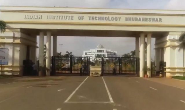
The choice of IIT Bhubaneswar as the site for this lab is strategic. Odisha has recently secured approvals for two major semiconductor projects under the India Semiconductor Mission: an integrated facility for Silicon Carbide (SiC)-based compound semiconductors and an advanced 3D glass packaging unit. IIT Bhubaneswar already hosts the Silicon Carbide Research and Innovation Centre (SiCRIC) and features existing cleanroom facilities, making it an ideal hub for expanding semiconductor research and skilling. The new lab will complement these assets, fostering collaborations with industry and supporting the development of talent for upcoming chip units nationwide.
Odisha Chief Minister Mohan Charan Majhi welcomed the approval, stating in a post on X (formerly Twitter):
I extend my sincere gratitude to Hon’ble Prime Minister Shri @narendramodi Ji and Union Minister for Electronics & IT Shri @AshwiniVaishnaw Ji for approving the ‘NaMo Semiconductor Laboratory’ at IIT Bhubaneswar.
With the Odisha Cabinet recently approving the State Semiconductor…
— Mohan Charan Majhi (@MohanMOdisha) October 5, 2025
Majhi further expressed confidence that the lab will inspire the youth, accelerate research, and elevate Odisha’s position on the national and global semiconductor map while advancing key national initiatives.
This development aligns with India’s ambitious semiconductor ecosystem growth, positioning the country as a key player in global chip supply chains amid rising demand for indigenous technology solutions.


